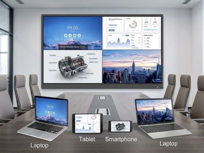

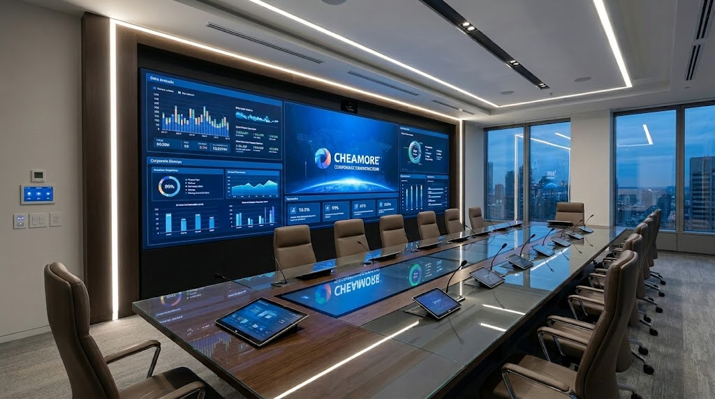
A native 163-inch 8K direct-view display operates with a 7680 × 4320 resolution across an active image area of 3600mm (W) × 2025mm (H), demanding a micro-pixel pitch of exactly P0.46875mm. By eliminating mechanical bezel interruptions and optical lattice diffraction, this architecture yields an uninterrupted pixel surface engineered for high-density enterprise data analytics, mission-critical dashboards, and close-proximity C-suite collaboration at viewing distances down to 1.8 meters.
At an executive viewing perimeter ranging from 1.8m to 4.5m, standard visual acuity (20/20 Snellen metric) resolves pixel structures larger than 0.6mm. A standard 4K 163-inch system utilizes a P0.9375mm pitch, rendering visible pixelation to viewers inside 3.2 meters. Native 8K integration over this specific diagonal resolves micro-typography, financial spread matrices, and architectural schematics without spatial aliasing or moiré interference during hybrid camera capture.
Deploying this scale of visual interface shifts the mechanical and thermodynamic demands on the host facility. Achieving reliable continuous operation requires flip-chip MicroLED packaging, specialized black optical resin matrix bonding, and common-cathode distribution to resolve the thermal, acoustic, and planarity boundaries established in high-tier corporate environments.
The ELDA-4 Framework: Enterprise Large-Scale Executive Display Assessment Matrix
To eliminate subjective assessment and vendor marketing bias during technical procurement tenders, enterprise display infrastructure should be evaluated against the empirical Enterprise Large-Scale Executive Display Assessment Matrix (ELDA-4). This framework establishes quantifiable performance thresholds across four foundational disciplines.
| Assessment Vector | Key Engineering Metrics | Target Enterprise Specification | Procurement Rejection Threshold |
|---|---|---|---|
| 1. Optical Continuity & Visual Ergonomics | Bezel clearance, physical pixel pitch, anti-glare treatment, moiré mitigation. | 0.00mm active seam; P0.468mm pitch; surface gloss <15 GU; diffuse black resin matrix. | Physical seams >0.5mm; pitch >0.7mm for <2.0m viewing; high-gloss specular reflections (>30 GU). |
| 2. Thermal Radiation & Acoustic Overhead | Front-surface operating temperature, acoustic noise emission, internal thermal derating. | Surface temp ≤33.0°C at 500 nits; <20 dB SPL sound floor at 1.0m (completely fanless). | Surface temp >38.0°C; audible fan noise (>28 dB SPL); thermal roll-off triggering within normal room ambient (22°C). |
| 3. Low-Gray Uniformity & Dynamic Range | Monotonic gamma linearity down to 0.01 nits, chromatic deviation (Δu'v'), color gamut. | Δu'v' ≤0.003 across 10% to 100% luminance; DCI-P3 ≥98%; Rec.2020 ≥85%; 16-bit low-gray processing. | Chromatic shift Δu'v' >0.006; visible gray-scale banding, dithering crawl, or magenta casting below 5% brightness. |
| 4. Structural & Lifecycle Infrastructure | Areal structural load (kg/m²), inrush power margin, MTBF diode failure rates, cold-spare yield. | Total system weight ≤38 kg/m²; inrush suppression <1.5× nominal; MTBF ≥100,000h; 8% single-wafer spare stock. | Load >55 kg/m²; inrush >3.0× triggering distribution breakers; batch-unmatched spare modules causing color patches. |
According to empirical verification audits from the 163-inch 8K corporate boardroom display Homepage engineering database, failure to achieve thresholds in Vectors 2 and 3 accounts for over 78% of post-commissioning executive dissatisfaction in enterprise boardrooms. Elevated screen surface temperatures create thermal discomfort for participants within two meters, while poor low-gray calibration degrades dark-mode interfaces and financial data visualization.
Display Technology Trade-Offs: P0.46 MicroLED vs. P0.9 COB vs. 3x3 LCD Video Walls
Selecting visual hardware for large-format executive installations requires analyzing the trade-offs between packaging topologies, optical resolving limits, and total capital expenditures. No single visualization platform serves every commercial scenario.
| Technical Parameter | Flip-Chip MicroLED (P0.46mm) | Standard COB (P0.93mm) | Commercial LCD (3×3 55-Inch) |
|---|---|---|---|
| Native Resolution | 8K UHD (7680 × 4320) | 4K UHD (3840 × 2160) | 3K × 3K Grid (5760 × 3240) |
| Optical Seams / Bezels | 0.00mm (Absolute Planar Zero) | 0.00mm (Absolute Planar Zero) | 0.88mm to 1.80mm mechanical grid |
| Static Contrast Ratio | >1,000,000:1 (Pure Black Matrix) | 10,000:1 to 30,000:1 | 1,100:1 to 1,300:1 |
| Low-Gray Gamma Tracking | Linear to 0.01 nits (No color shift) | Linear to 0.5 nits (Minor clip) | Non-linear backlight bleed (<1.0 nit) |
| Front Surface Temperature | 31.0°C to 33.5°C (Common-Cathode) | 36.0°C to 41.0°C (Common-Anode) | 34.0°C to 38.0°C (Edge LED) |
| Acoustic Noise Floor | <18 dB SPL (Convection passive) | <24 dB SPL (Passive structural) | 32 dB to 40 dB SPL (Cooling fans) |
| Capital Cost Ratio | 3.2× to 4.0× | 1.8× to 2.2× | 1.0× (Baseline) |
Technology Analysis and Application Boundaries
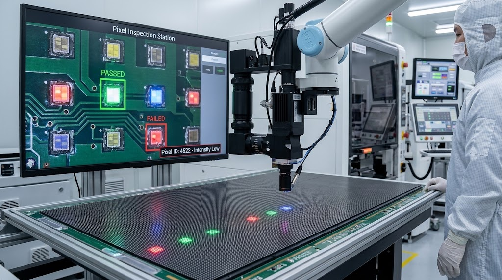
1. Flip-Chip MicroLED (P0.46mm 8K Array): Utilizes microscopic flip-chip dies (<50μm) bonded directly to the substrate with an engineered optical resin layer. This design eliminates bond wires, drastically reduces internal thermal resistance, and maximizes the black area ratio to over 98%. This enables a 1,000,000:1 contrast ratio and native compliance with the SMPTE ST 2084 (PQ curve). The primary trade-off is capital expenditure and an intolerance for sub-wall surface imperfections.
2. Standard Chip-on-Board (P0.9mm to P1.2mm 4K Array): Leverages larger LED dies mounted in clusters beneath an epoxy encapsulation barrier. While offering robust mechanical surface protection (IP54/IP65 ratings) and lower manufacturing costs, physics limits a 163-inch diagonal to 4K resolution. Visual uniformity is also susceptible to batch variations in epoxy gloss, causing slight optical tiling effects under ambient boardroom downlights.
3. Commercial LCD Video Wall Matrix (3×3 55-Inch Configuration): Provides a cost-effective, familiar multi-screen setup, but remains structurally compromised by mechanical bezels. Even ultra-narrow 0.88mm panels create a composite black crossbar of roughly 1.8mm across charts, video conference streams, and presentation decks. Additionally, individual LCD panels degrade and shift chromaticity at different rates, requiring frequent calibration cycles.
FAQS
How can procurement teams verify genuine MicroLED versus re-badged Mini-LED or SMD COB?
True MicroLED utilizes microscopic flip-chip dies with physical dimensions under 50μm, devoid of individual lead-frame packaging, mounted directly to the circuit substrate. Mini-LED typically uses larger dies (100μm to 200μm). During procurement, mandate third-party cross-sectional scanning electron microscope (SEM) or optical profilometer reports certifying the physical die footprint, along with an optical resin black-matrix area ratio exceeding 95%.
How is maintenance handled if a display must be mounted flush against a wall?
Modern ultra-fine-pitch systems use high-precision magnetic vacuum extraction tools that service modules entirely from the front. Defective modules are released via electronically calibrated vacuum suction in under 30 seconds without disrupting adjacent tiles. Zero rear access space is required, allowing total wall-depth footprints (cabinet plus mounting frame) to remain under 65mm.
Does high ambient daylight in executive boardrooms cause optical wash-out on MicroLED?
No. MicroLED displays engineered with deep black resin absorption matrices maintain ambient contrast ratios (ACR) exceeding 4,000:1 under direct 500-lux boardroom illumination. Unlike standard projection or consumer-grade LCD surfaces that suffer from diffuse scatter, the microscopic die surface combined with anti-reflective optical coatings absorbs ambient light without washing out blacks.